What Is Semiconductor Manufacturing Equipment? A Guide to Types, Roles, Key Makers, and the Semiconductor Process Flow
Semiconductors are built into virtually every product—from smartphones to automotive systems. To manufacture them, highly specialized equipment is used, with each tool playing a different role depending on the process step.
This article explains, in an easy-to-follow way, the basic types of semiconductor manufacturing equipment and their roles, the overall process flow, and the latest landscape of major equipment manufacturers.
Table of Contents
Semiconductor Manufacturing Equipment Basics and Roles | Why Process-Specific Tools Matter
Semiconductor manufacturing equipment refers to a set of specialized machines used throughout the series of processes that turn a silicon wafer into computer chips (integrated circuits).
Microchips used in smartphones and PCs contain tens of billions of tiny transistors, and manufacturing them requires hundreds of process steps and many different types of equipment.
Because the manufacturing process is extremely complex, dedicated tools and materials optimized for each step are essential.
There are tools designed specifically for each task—such as drawing ultra-fine circuit patterns on a wafer, stacking thin layers of material, and removing unwanted portions.
Advances in semiconductor manufacturing equipment have helped sustain Moore’s law (the idea that the number of components per integrated circuit doubles roughly every two years), playing a critical role in the evolution of semiconductor technology.
Key Types of Semiconductor Manufacturing Equipment and How They Work | A Summary by Process Step
Semiconductor manufacturing is divided into several major steps, and each step has corresponding equipment. Below are representative tool categories and their roles.
What Is Photolithography? How Exposure Tools Work and Why They Matter
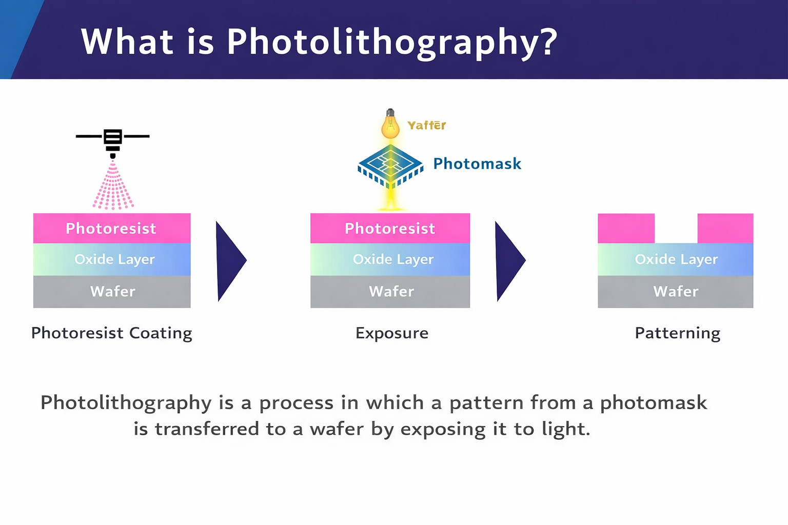
Photolithography is the process of projecting light through a photomask onto a wafer to transfer a circuit pattern onto the wafer.
A lithography tool irradiates a wafer with ultraviolet light that passes through a photomask (the master plate carrying the chip’s circuit layout), transferring an ultra-fine circuit pattern onto a photosensitive material (photoresist).
After exposure, development forms the circuit pattern in the resist, and subsequent etching processes machine the substrate according to that pattern.
Photolithography is a key step that determines a chip’s line width (minimum pattern dimension). State-of-the-art tools can transfer extremely fine patterns by using shorter-wavelength light such as extreme ultraviolet (EUV).
What Is the Role of Etching Tools? The Essential Material-Removal Step for Circuit Formation
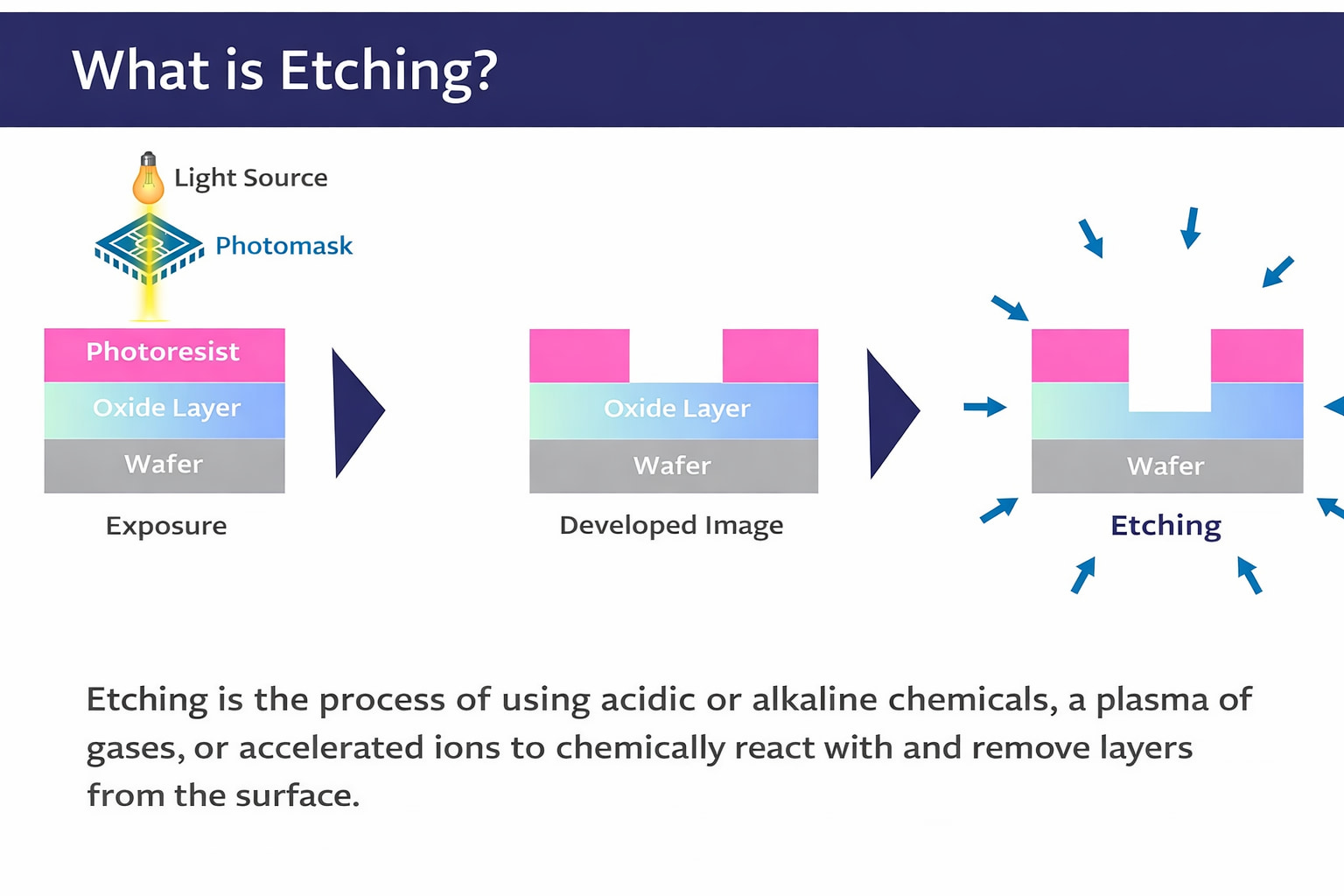
Etching tools are used to remove unwanted thin films or materials.
After a pattern is created by photolithography, the etching tool selectively removes exposed areas of thin film or the substrate, forming the three-dimensional structure of the circuit.
Etching includes wet etching, which dissolves material using liquid chemicals, and dry etching (such as reactive ion etching), which removes material in the gas phase using plasma and related methods. The right approach is chosen depending on the purpose.
For example, in today’s advanced nodes, dry etching is used primarily; ions in the plasma precisely remove material from the wafer surface to create fine structures.
What Are Deposition Tools? Explaining the Differences and Mechanisms of CVD, PVD, and ALD
Deposition tools are used in the process of forming new layers as thin films on a wafer.
They deposit thin films—such as silicon oxide films and metal films that become materials for semiconductor circuits—uniformly across the entire wafer.
There are multiple deposition techniques. Typical examples include chemical vapor deposition (CVD), which uses chemical reactions of gases, and physical vapor deposition (PVD), which vaporizes and ejects material in a vacuum.
For instance, sputtering (a type of PVD) forms a thin film by bombarding a target metal with ions to eject atoms, which then adhere to the wafer at the atomic level.
In recent years, atomic layer deposition (ALD)—which enables thickness control at the atomic-layer level—has also been used.
In deposition steps, thin films of various materials—such as functional layers and interconnect layers—are stacked one by one.
Switches for High Vacuum Class
- GN Switches -
High vacuum at 10-5Pa with low outgassing
Click here ›How Wafer Cleaning Tools Work—An Essential Step Between Processes
These tools are used to wash away contamination and particles from the wafer surface.
In semiconductor manufacturing, even tiny dust or impurities can cause circuit defects, so wafers are cleaned with washing tools between process steps.
Using chemical solutions and ultrapure water, these systems remove nanometer-scale particles, organic and metal residues, and even native oxide films.
A representative method is RCA cleaning (a sequence cleaning process using chemical solutions). In addition, because the surface must be fully dried for the next step, spin drying and related drying methods are also used.
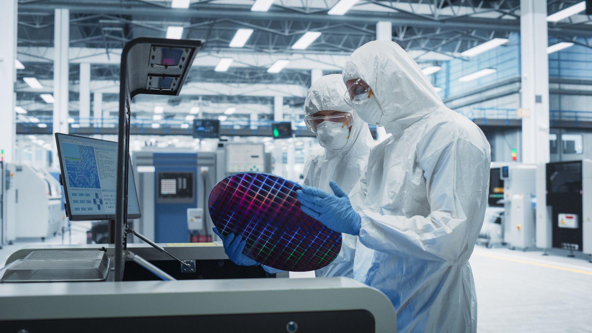
Types and Features of Inspection Tools for Dimensional / Film-Thickness Metrology and Defect Detection
These are tools that measure wafer and circuit-pattern dimensions and film thickness, and inspect for defects.
To confirm whether exposure and etching achieved the intended results—and whether fine patterns have misalignment or defects—various metrology and inspection steps are performed between processes.
For example, visual inspection systems using optical microscopes or electron beams detect tiny pattern defects, while film-thickness metrology tools such as ellipsometers precisely measure the thickness of oxide films and photoresist.
Process control enabled by inspection and metrology tools—early detection of process variation and abnormalities—is essential to improving yield. Especially as circuits continue to scale, specialized manufacturers represented by KLA provide advanced inspection technologies.
As described above, semiconductor manufacturing relies on dedicated equipment for each process step.
For example, photolithography includes not only the exposure tool but also a coater/developer system that applies and develops photoresist. Likewise, even within “etching,” there are many variations depending on the gases used and the etching method inside the tool.
By operating these tools in coordination and processing wafers step by step, it becomes possible to build complex integrated circuits.
What Is the Front-End Process in Semiconductor Manufacturing? Tool Order and Roles Explained Clearly
The front-end process (wafer process) advances by repeating the steps performed by the equipment described above many times.
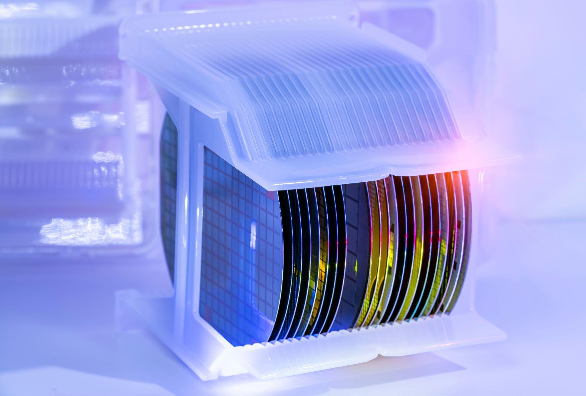
First, a silicon wafer substrate of about 300 mm in diameter is prepared, and various thin films are deposited to build the base layers.
Next, photoresist is applied across the wafer, and the circuit pattern is exposed using a photolithography tool. After development, the pattern appears in the resist; that pattern is then used as a mask as an etching tool processes the thin film to form the circuit layer.
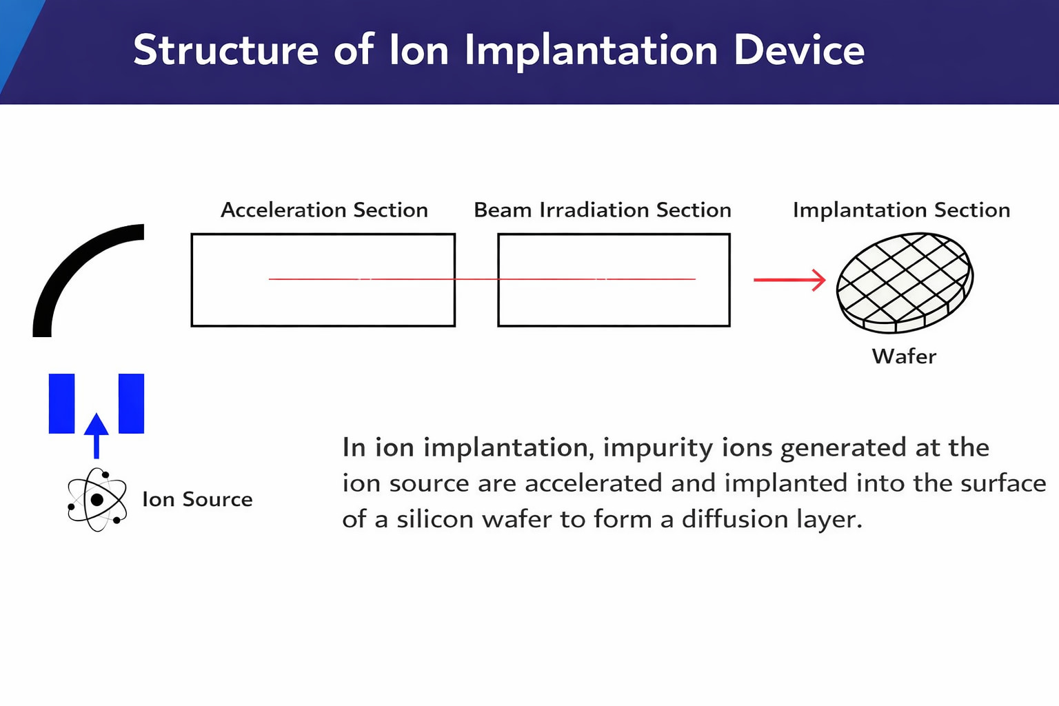
As needed, an ion implantation tool introduces impurities into specific areas to give the transistor its electrical characteristics.
After each step, cleaning tools wash away unwanted resist residue and particles to prepare for the next process.
By repeating the cycle of deposition → lithography → etching → (implantation) → cleaning for each layer, multi-layer circuits are built up.
In advanced microprocessors, the photolithography cycle may be repeated roughly around 50 times on a single wafer, bringing the total number of process steps to the hundreds.
At the end of the manufacturing flow, the entire wafer is inspected and only good dies are selected.
The wafer is then singulated into individual chips using a dicing tool, followed by back-end steps such as mounting onto a package substrate and bonding (interconnect wiring).
Finally, completed chips are electrically tested again, confirmed to be defect-free, and shipped.
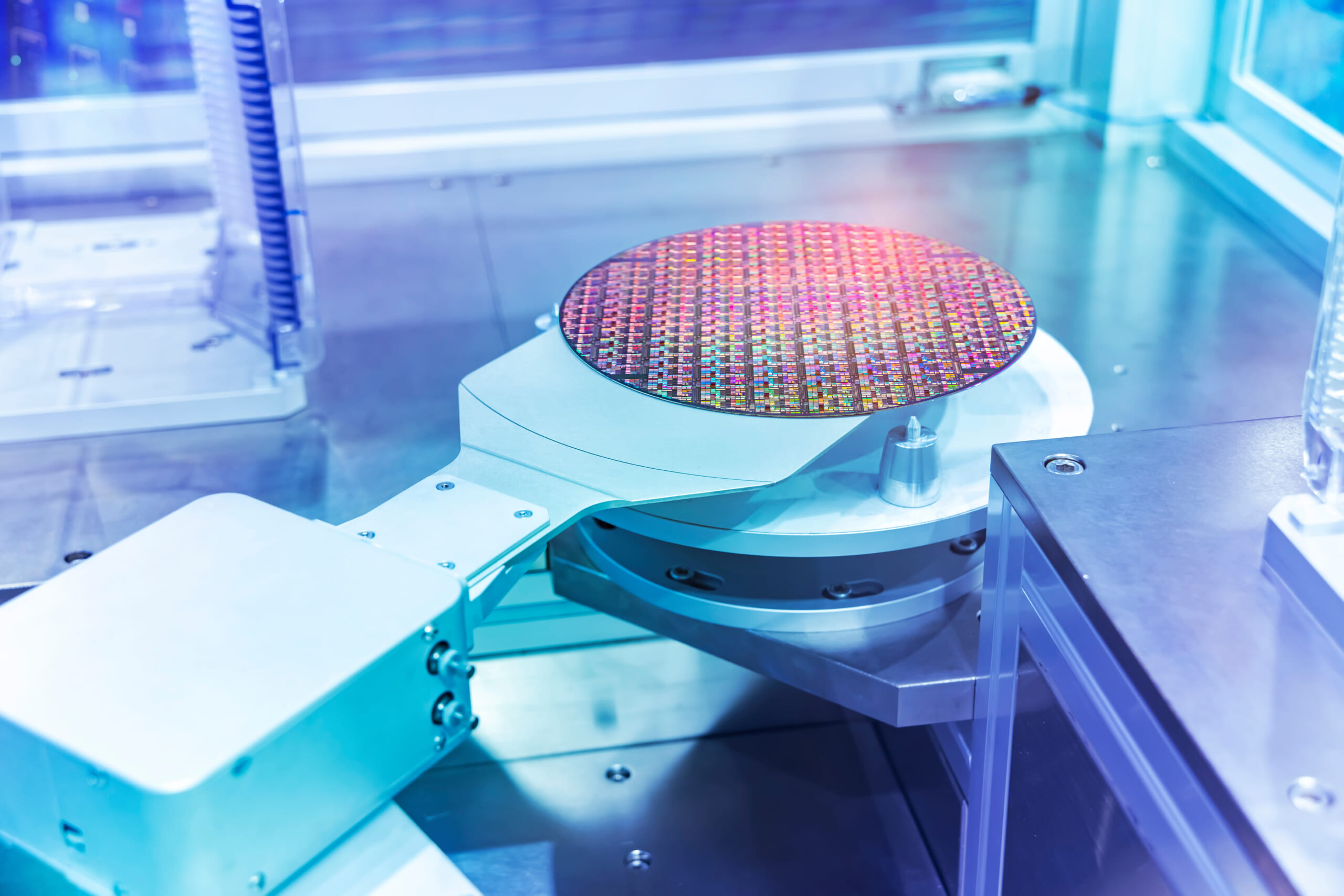
In general, front-end manufacturing tools are lined up throughout a cleanroom, and wafers are transported to each tool in sequence by automated handling systems (robot arms and transport carts).
Because these processes are operated through control systems and people do not directly touch the equipment, a high level of cleanliness is maintained in the cleanroom.
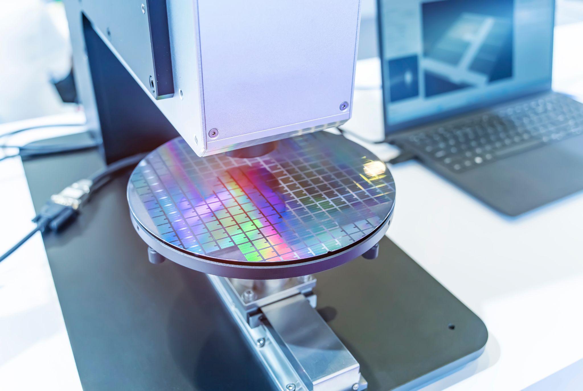
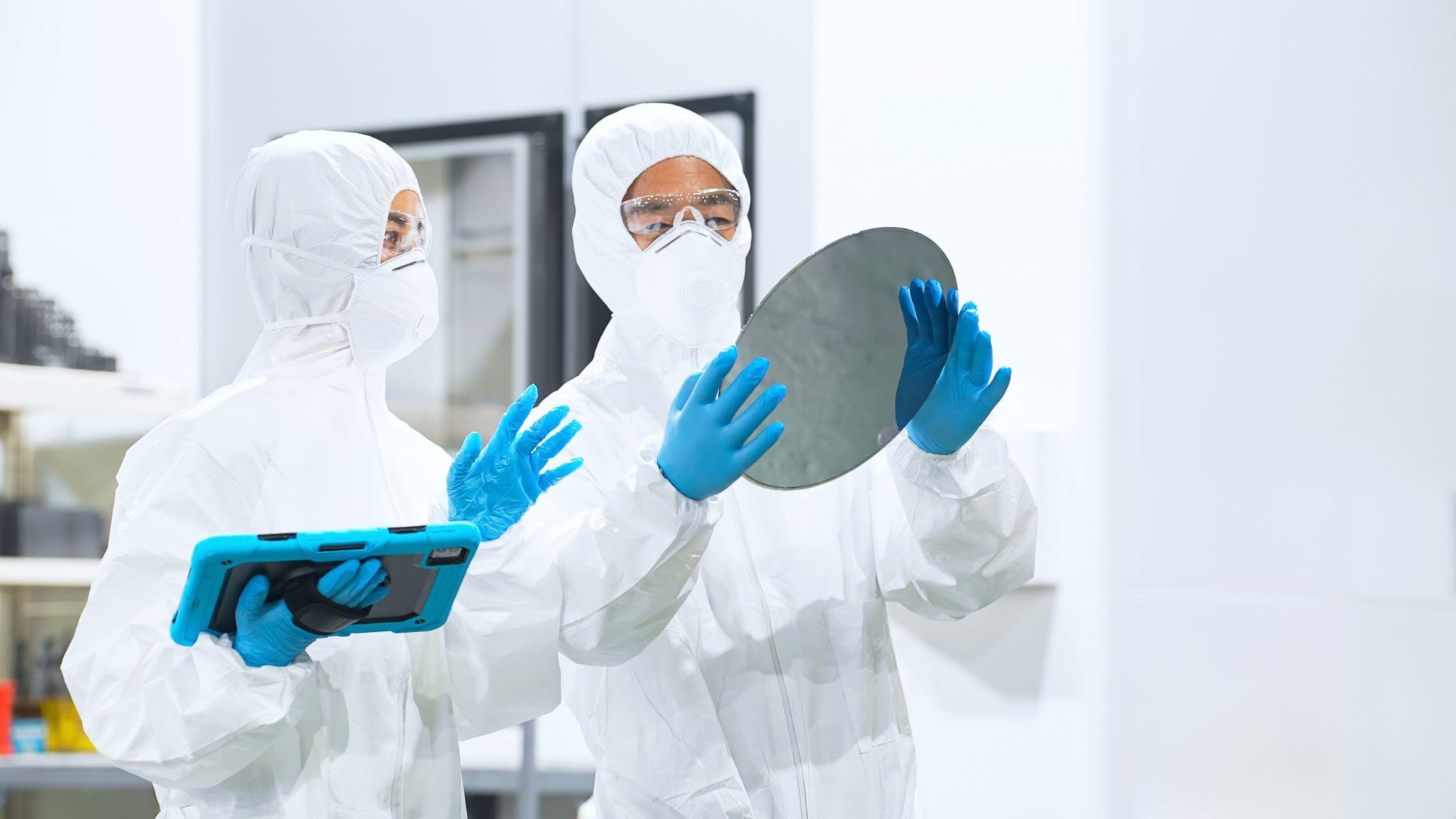
The wafer surface has many stacked films and often appears iridescent due to light reflection. By repeating photolithography and etching on the wafer, ultra-fine circuit patterns are formed.
High Precision Positioning
- MT-Touch Switches -
0.5 μm repeatability without amplifier IP67, highly resistant to adverse environments
Click here ›Major Companies in the Semiconductor Equipment Industry | Who Are the Global Leaders Like ASML and TEL?
The semiconductor equipment industry is highly specialized and concentrated, with only a handful of top companies holding large global market shares.
Below are major semiconductor manufacturing equipment makers.
| Company | Country |
|---|---|
| Applied Materials | United States |
| Lam Research Corporation | United States |
| KLA Corporation | United States |
| Teradyne | United States |
| Plasma-Therm | United States |
| ASML | Netherlands |
| Tokyo Electron Limited (TEL) | Japan |
| SCREEN Holdings Co., Ltd. | Japan |
| Advantest Corporation | Japan |
| Hitachi High-Tech Corporation | Japan |
These are major players overall, and each has its own areas of strength.
For example, ASML specializes in lithography and is the only company in the world that supplies state-of-the-art EUV lithography tools.
Applied Materials and Lam Research offer broad product portfolios in deposition and etching, and Lam Research in particular has a strong market presence in plasma etching tools.
Tokyo Electron is one of Japan’s leading equipment makers, with a wide lineup spanning deposition and etching, as well as coater/developer systems (photoresist coating and developing tools) and cleaning tools.
Tokyo Electron holds an almost dominant global share in photoresist coater/developer systems and, together with ASML’s EUV scanners, supports leading-edge chip manufacturing.
In the inspection equipment segment, U.S.-based KLA stands out and provides metrology and inspection technologies essential for yield management.
In terms of market structure, these top five companies (Applied Materials, ASML, Tokyo Electron, Lam Research, and KLA) account for a large portion of the global semiconductor equipment market. Some companies hold an almost exclusive position in a specific field (such as ASML in lithography), while others—like Applied Materials and Tokyo Electron—cover multiple equipment categories.
Because the equipment industry is closely tied to national strategies, companies in Europe, the U.S., and Japan with advanced technologies remain central players. However, in recent years, government support programs and new entrants have been changing the competitive landscape.
Even so, developing cutting-edge equipment still requires massive investment and years of accumulated expertise, making new entry difficult and maintaining an oligopolistic structure dominated by top companies.
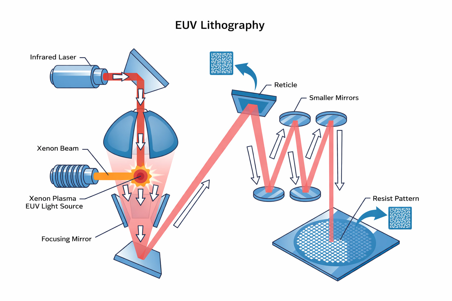
What Is EUV Lithography? How Advanced Semiconductor Tools Evolved to Enable Leading-Edge Chips
Advances in semiconductor manufacturing equipment have enabled chips to become smaller and more powerful.
A representative example is the commercialization of EUV lithography (extreme ultraviolet lithography).
EUV lithography transfers circuit patterns using 13.5 nm light (extreme ultraviolet), which has a much shorter wavelength than conventional methods, enabling extremely fine patterning at just a few nanometers in width.
With immersion ArF excimer lasers (193 nm wavelength), the industry had been approaching physical limits and further scaling became difficult. The emergence of EUV exposure tools has enabled leading-edge chip production in the 5 nm and 3 nm generations.
ASML’s EUV lithography tool—commercialized after roughly two decades of R&D—is a massive and highly precise machine, often said to cost tens of billions of yen per unit, and it incorporates unprecedented technical challenges such as operating reflective optics in ultra-high vacuum.
As a result, the success of EUV tools has extended the life of semiconductor scaling (Moore’s law), enabling smartphones and CPUs to achieve remarkable transistor density.
Innovation beyond lithography also supports semiconductor progress. For example, in deposition, the adoption of ALD—capable of controlling film thickness at the atomic level—has improved transistor performance. In etching as well, new approaches have been developed to selectively and rapidly remove only specific materials.
With the rise of three-dimensional device structures (such as FinFETs and stacked NAND flash architectures), equipment has also evolved to process and measure complex 3D geometries that differ from traditional planar structures.
For example, in NAND flash, stacking more than 100 memory cell layers requires etching extremely deep holes (vias). Equipment technology that enables high-aspect-ratio etching is a key enabler.
In short, progress in semiconductor chips cannot be discussed without innovation in semiconductor manufacturing equipment.
To meet next-generation demands, equipment makers continue daily development—improving resolution through higher-NA (numerical aperture) light sources and supporting new materials and new processes.
Further performance gains in the electronic devices we use every day depend on something we rarely see: cutting-edge semiconductor manufacturing equipment operating inside cleanrooms.
Switches for High Vacuum Class
- GN Switches -
High vacuum at 10-5Pa with low outgassing
Click here ›Practical Notes on Semiconductor Manufacturing Equipment Based on Shop-Floor Experience
Here, we explain the differences between machining parts for semiconductor manufacturing equipment and machining parts for general-purpose industrial machinery.
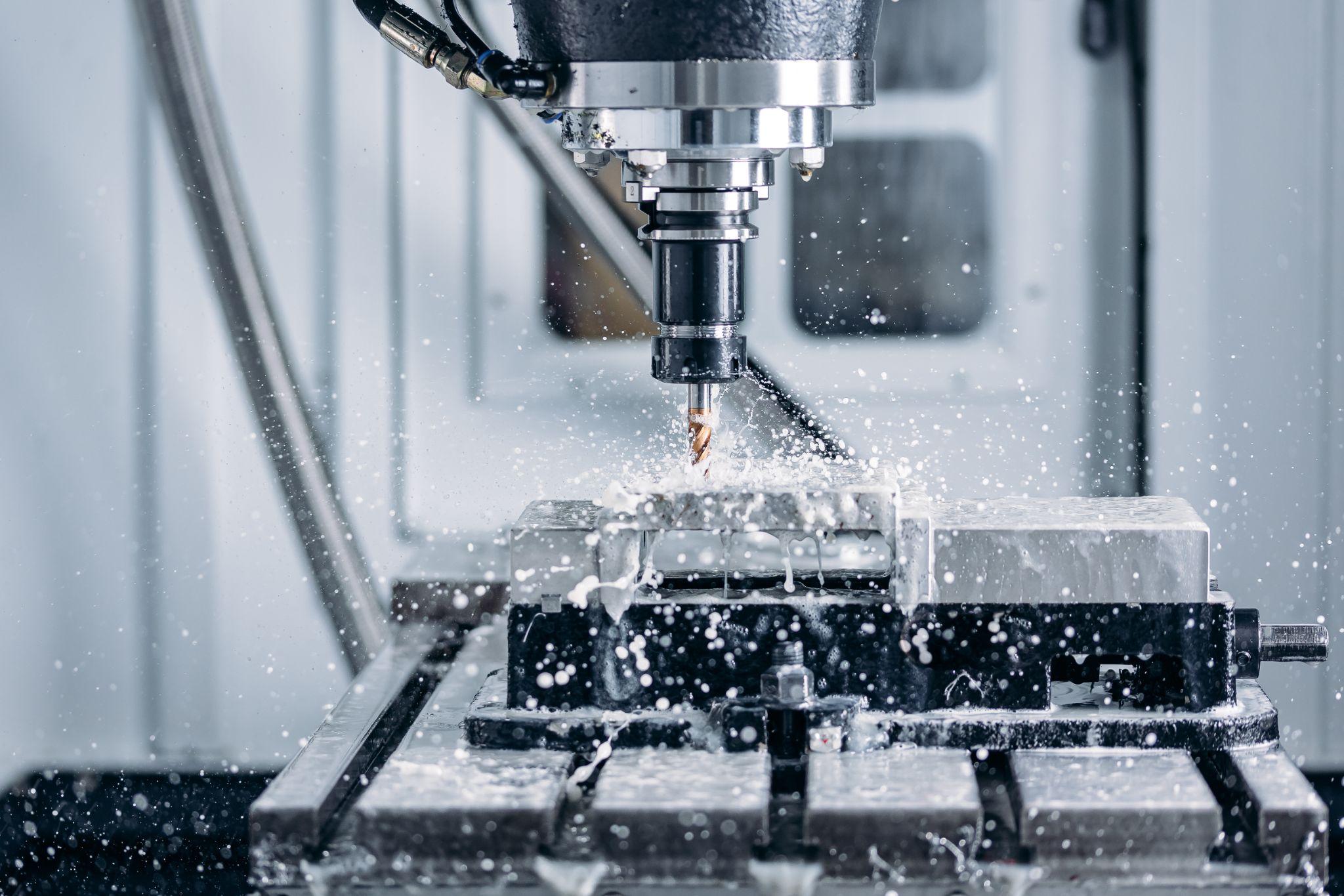
Why Semiconductor Equipment Parts Are Difficult to Machine | High Precision × Difficult-to-Cut Materials
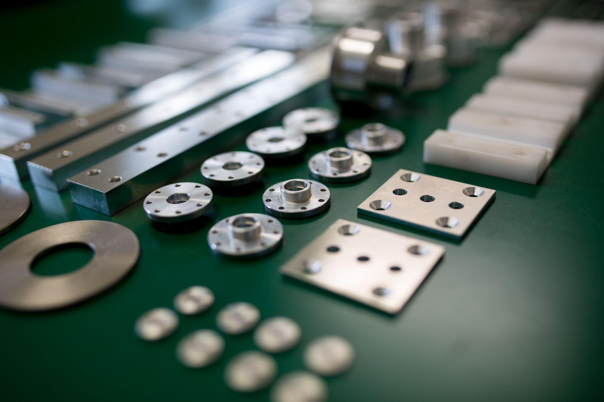
Parts for semiconductor manufacturing equipment are often made from materials that are harder and more durable than those used for typical machine parts.
Below are examples of difficult-to-cut materials commonly used for semiconductor equipment parts.
- Titanium alloys
- Stainless steel alloys
- Inconel
- Aluminum alloys (1000, 4000, 6000 series)
- Hastelloy
In addition to very demanding dimensional accuracy, surface finish, and geometric tolerances, stable mass production is essential—so facilities and environments capable of consistently producing high-precision parts are required.
All of these materials cause severe tool wear, and even small environmental changes (such as temperature or coolant concentration) can shift machined dimensions—driving machining costs higher.
Moreover, because required tolerances are far tighter than those for general manufacturing equipment, 100% inspection at all required locations becomes necessary—adding not only machining cost but also significant labor and resource costs for inspection.
For these reasons, machining parts for semiconductor manufacturing equipment demands an even higher level of capability than machining parts for typical manufacturing equipment.
Is Machining Accuracy Determined by the Machine Tool? Required Machine Performance for Semiconductor Parts
Machine tools have strengths and weaknesses depending on their intended use. Some are highly rigid and excel at heavy cutting, while others specialize in precision machining using small tools at very high spindle speeds (tens of thousands of rpm).
Machines used to make semiconductor equipment parts are typically in the latter category. And as explained by the “mother machine principle,” it is impossible to machine parts more accurately than the machine’s own accuracy.
Therefore, it is recommended to use machine tools whose accuracy exceeds the accuracy required by the semiconductor equipment parts being produced.
Machines routinely used for heavy cutting with large-diameter tools—or machines that have degraded over time and can only maintain general machine accuracy—cannot meet the required precision. If you use them, limit them to roughing or parts that do not require high precision.
Although using more machines increases equipment needs, workload, and labor costs, separating machines dedicated to finishing is recommended because it is an essential approach for maintaining stable high accuracy.
What Is the “Mother Machine Principle”?
The “mother machine principle” states that the accuracy of a machined part depends on the accuracy of the machine tool used to produce it.
If the machine tool’s accuracy is low, it cannot achieve the required dimensional accuracy or geometric tolerance. In an extreme example, a machine with excessive play cannot meet tight requirements even with high-precision tools—because no part can be machined more accurately than the machine itself.
For parts that require tight accuracy, dimensional tolerances, and geometric tolerances—such as semiconductor equipment parts—use machine tools capable of high-accuracy machining.
High-precision seating confirmation of workpiece and jig
- Air Gap Sensor -
You can check not only "presence/absence" but also "adhesion (gap)" at the same time with a repeatability of ±0.5 μm.
Click here ›Why “High Precision for Everything” Is Not OK | The “Right Material in the Right Place” Approach
Many parts used in semiconductor equipment are high-precision, hard, durable, and corrosion-resistant—but not every part requires the same level of accuracy, hardness, or corrosion resistance.
For example, parts used in semiconductor cleaning may require high corrosion resistance. However, in a unit (base plate) that controls the flow rate of cleaning liquid, extremely high corrosion resistance may not be necessary—so commercially available screws can often be used to mount the base plate.
Requiring high precision for every part drives costs up unnecessarily. It also increases equipment build time, which can prevent delivery within the required timeframe and risk lowering customer satisfaction.
When machining parts, understanding the application and purpose—such as “where in the machine will this part be used?” and “why does it require high precision?”—makes it possible to reduce manufacturing cost and lead time.
It also enables you to select an appropriate machine tool based on the required accuracy, allowing the part to be produced in an environment suited to its needs.
What Are Metrol’s High-Precision Positioning Sensors?
In machining semiconductor equipment parts, accuracy on the order of ± several microns is required, and even slight misalignment can directly lead to serious defects and higher costs.
That is why precise control of machining position and reliable detection of workpiece seating are critically important.
Metrol’s high-precision sensors are trusted in these precision machining environments.
With a lineup ranging from contact-type to non-contact sensors, they address a wide range of shop-floor needs—helping reduce setup time, improve quality, and cut defects.
Below, we introduce representative products that can support machining processes and equipment design.
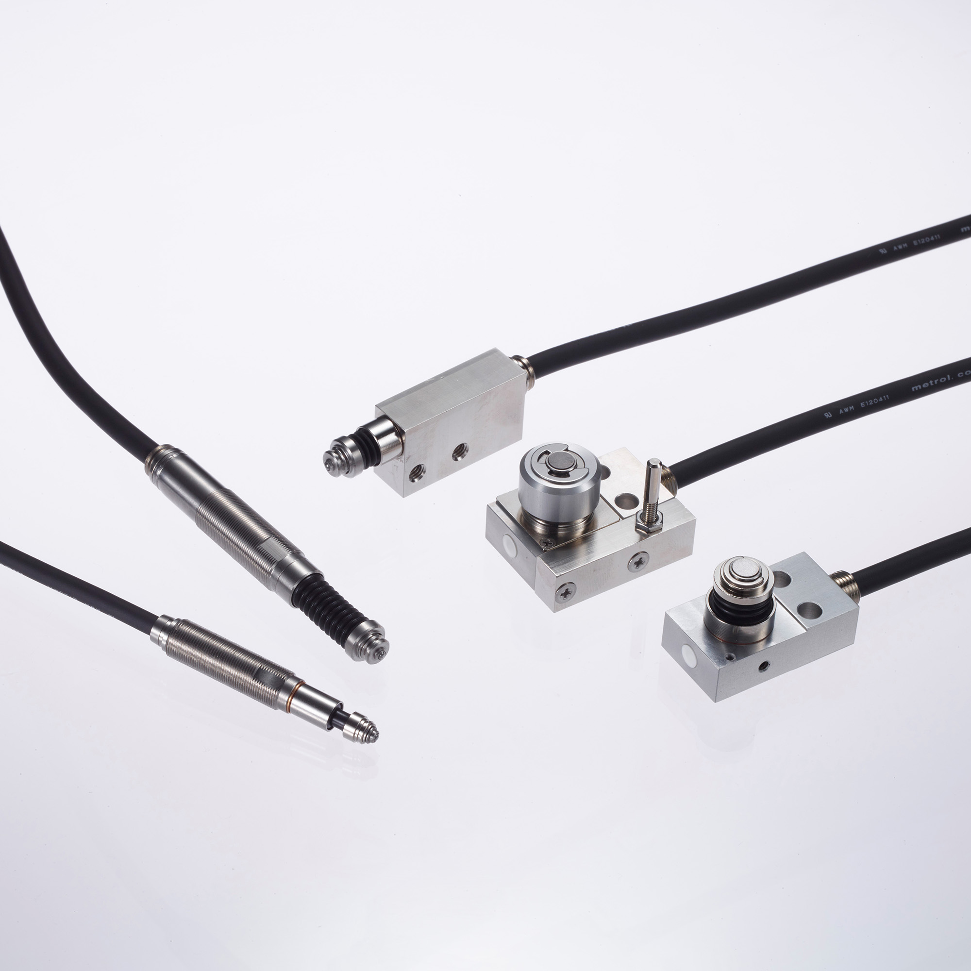
High-Precision Positioning Touch Switches
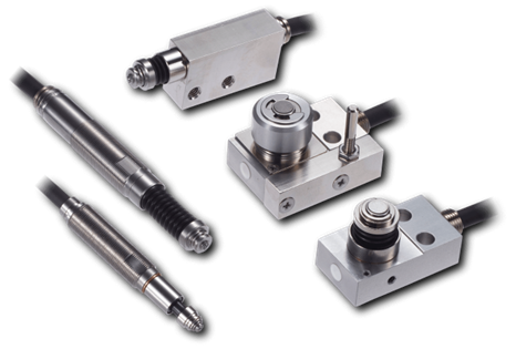
These are contact-type high-precision switches used for positioning and workpiece presence detection in machine tools, robots, and jigs. They achieve an extremely high repeatability of up to 0.5 µm and feature IP67-rated waterproof and dustproof protection, ensuring stable operation even in harsh environments. With more than 200 standard models available, they offer a wide range of variations, including designs for confined spaces, high-temperature environments, vacuum applications, and low contact force requirements.
Tool Setter (Tool Length Measurement Sensor)
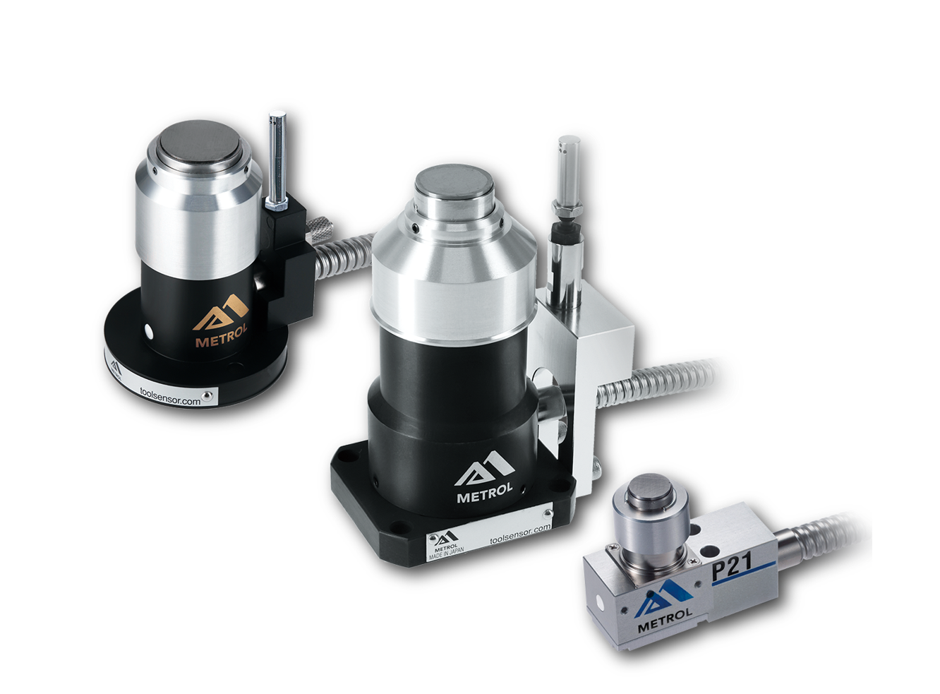
This is a contact-type sensor installed on CNC machine tools and industrial robots for tool length measurement, reference position setting, and tool breakage detection. By automatically measuring and compensating for tool length, wear, and thermal displacement inside the machine, it helps prevent machining defects and significantly reduces setup time. It is one of Metrol’s best-selling products, with a proven track record of more than 500,000 units shipped in 74 countries worldwide.
Touch Probe (On-Machine Measurement Probe)
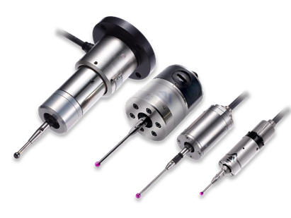
This is a contact-type probe for in-machine measurement, installed on machine tools and robots to automatically perform workpiece positioning (centering) before machining and dimensional measurement after machining. With a repeatability of 1 µm, it automates workpiece referencing and dimensional inspection, replacing skilled manual operations to reduce setup time and help prevent machining defects. Both wired and wireless models are available, meeting retrofit needs for 5-axis machining centers and robotic applications.
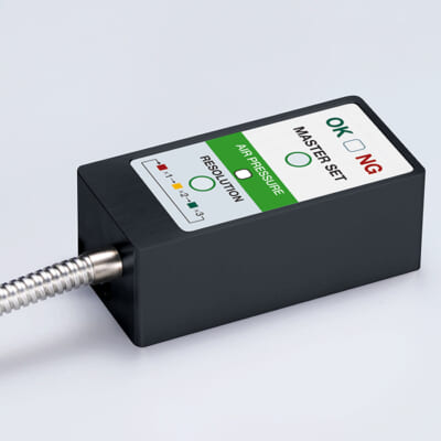
Air Gap Sensor (Pneumatic Sensor)
This is a non-contact sensor that uses air pressure to detect workpiece seating conditions with micron-level accuracy. It can detect gaps (“lift”) of less than 10 µm—previously difficult to measure—with a repeatability of ±0.5 µm, helping prevent machining defects and equipment downtime caused by insufficient contact between the workpiece and fixture. The sensor is used in applications such as semiconductor manufacturing processes, precision part clamping operations, and grinding wheel positioning on grinding machines, and it is a smart sensor that also supports the international standard IO-Link communication.