What Is a Semiconductor Wafer?
Key Points
- Semiconductor wafers are the foundation of IC chip manufacturing and are indispensable for electronic devices.
- Manufacturing involves highly precise multi-step processes.
-
Larger wafer sizes, new materials, and environmental initiatives are key future trends.
Table of Contents
What Is a Semiconductor Wafer?
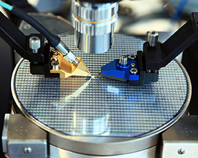
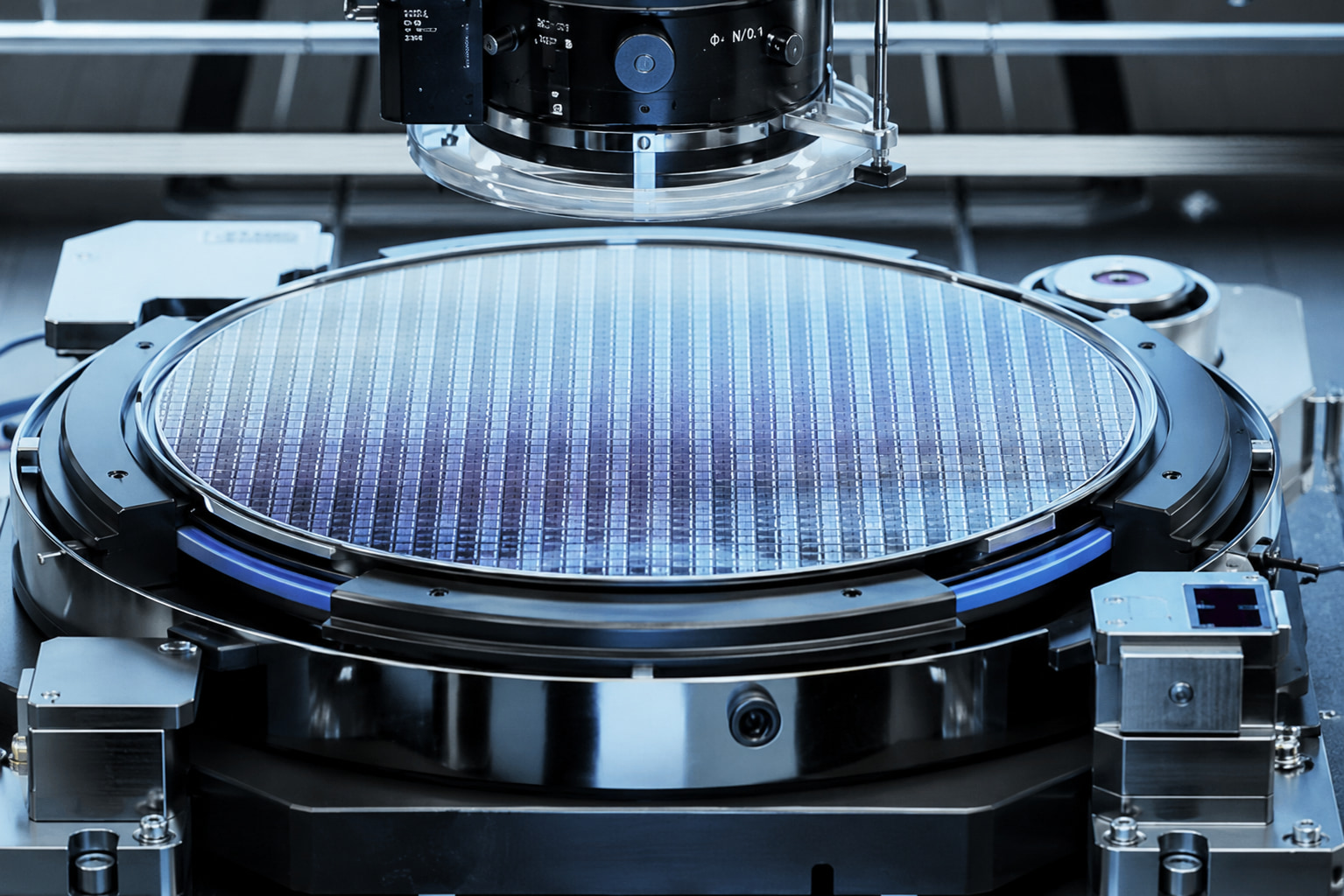
A semiconductor wafer is a disk-shaped substrate made from semiconductor materials such as silicon and serves as an essential foundation for modern electronic devices. In the past, wafers with diameters of approximately 100mm (4 inches) were standard, but today 200mm (8-inch) and 300mm (12-inch) wafers are the mainstream. Practical adoption of 450mm wafers is also being considered for the future. Larger wafer diameters enable more chips to be produced from a single wafer, improving productivity and cost efficiency.
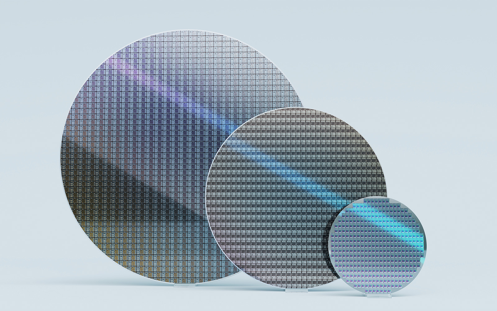
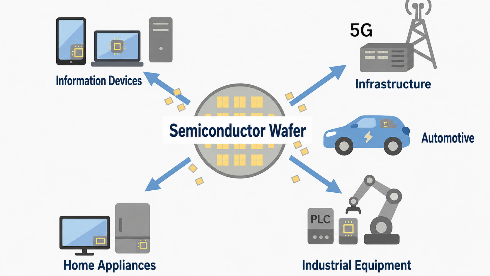
Numerous microscopic circuits are formed on these disk-shaped wafers, from which individual chips such as ICs and LSIs are cut out. Semiconductors used as the core components of electronic devices essential to daily life and industry—including smartphones, computers, home appliances, automobiles, and industrial robots—are all manufactured from these wafers.
Silicon is the most commonly used material for semiconductor wafers. Because silicon is abundant in the Earth's crust, inexpensive, and possesses excellent electrical properties, it has become the primary material in the semiconductor industry. In particular, highly purified single-crystal silicon offers excellent uniformity in electrical characteristics and is essential for manufacturing high-performance semiconductor devices.
Switches for High Vacuum Class
- GN Switches -
High vacuum at 10-5Pa with low outgassing
Click here ›Applications and Importance of Semiconductor Wafers
Semiconductor wafers support core technologies across virtually every sector of modern society. Their main applications are as follows.
1. Information Technology Equipment
IT equipment such as computers, smartphones, and servers contains an enormous number of semiconductor chips. Components responsible for core data processing functions—including CPUs, GPUs, memory devices, and storage controllers—are all manufactured from wafers.
2. Home Appliances
Household appliances such as televisions, refrigerators, washing machines, and air conditioners also incorporate numerous control ICs and sensors, all of which are made from semiconductor wafers.
3. Automotive and Mobility Sector
With the rise of EVs (electric vehicles) and autonomous vehicles, the number of semiconductors installed in a single vehicle has increased dramatically. Semiconductors are used in a wide range of systems, including engine control, power management, and ADAS (Advanced Driver Assistance Systems), contributing to improved safety and efficiency.
4. Industrial Machinery and Robotics
FA (Factory Automation) systems and industrial robots that support factory automation also rely heavily on semiconductor chips for sensing, motion control, and communication functions.
5. Infrastructure and Telecommunications
Semiconductors are indispensable for the infrastructure supporting high-speed, high-capacity communications such as 5G, data centers, and AI processing. Demand for semiconductors is expected to continue growing with the expansion of IoT and smart cities.
In this way, semiconductor wafers form the foundation of modern hardware and are closely linked to the advancement of society as a whole.
Semiconductor Wafer Manufacturing Process
Semiconductor wafer manufacturing consists of numerous highly advanced precision processes. The major processes are explained below.
1. Ingot Manufacturing (Single-Crystal Growth)
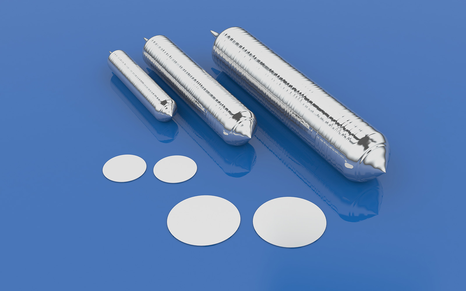
Silicon raw material (polycrystalline silicon) is melted at high temperatures, and single-crystal silicon ingots (cylindrical crystals) are grown using methods such as the Czochralski process. Because these single crystals determine the electrical characteristics of the wafer, extremely high purity and crystal quality are required.
A manufacturing method in which a crystal “seed” is inserted into the molten material and slowly rotated while being pulled upward to form a large rod-shaped crystal (ingot).
2. Wafer Slicing
The ingot is sliced into disk-shaped wafers with a thickness of several hundred microns. At this stage, the wafer has been formed, but its surface remains rough and uneven.
3. Polishing and Mirror Finishing
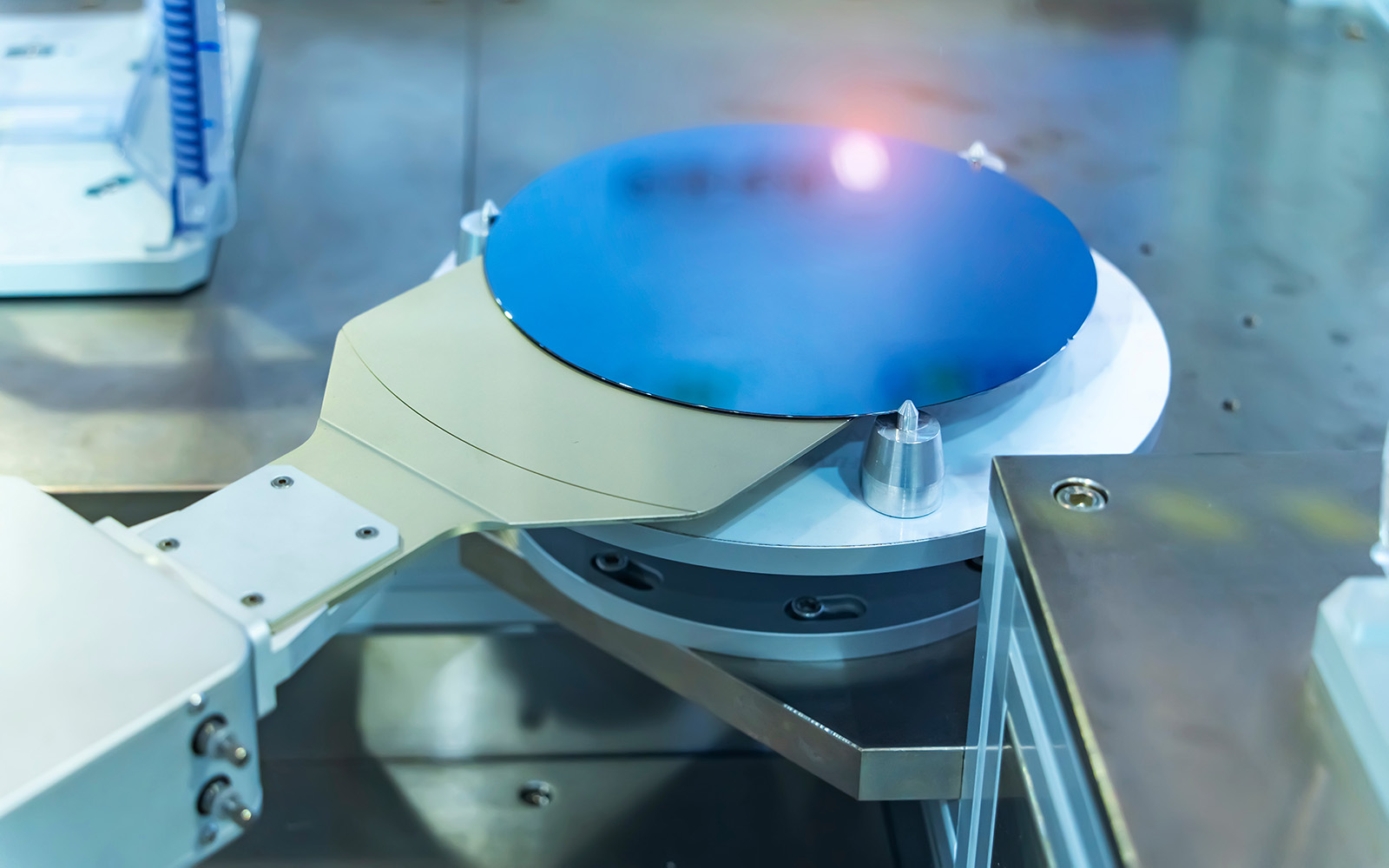
The wafer surface is chemically and mechanically polished using CMP (Chemical Mechanical Polishing) to achieve nanometer-level flatness and mirror-like smoothness. This is an extremely important step for forming fine patterns in subsequent processes.
4. Cleaning and Inspection
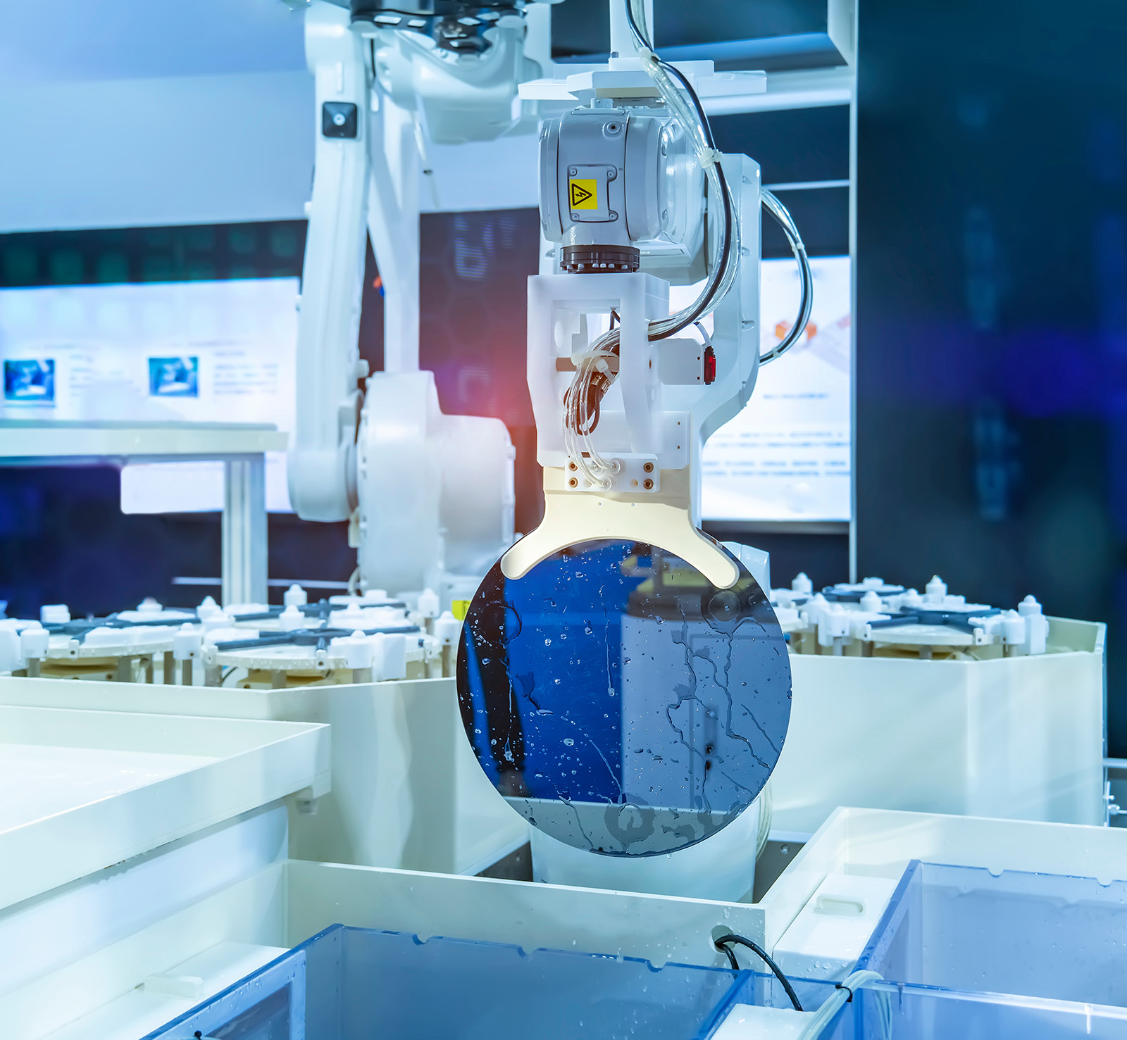
To remove microscopic dust and contaminants, wafers are thoroughly cleaned using ultrapure water and chemicals. Surface defects, particles, and thickness variations are then inspected with high precision to eliminate defective products.
5. Device Fabrication Process
The completed wafer is then transferred to IC fabrication processes such as photolithography, etching, ion implantation, and thin-film deposition, where complex circuits are formed on the wafer surface. At this stage, hundreds to thousands of chips are manufactured on a single wafer.
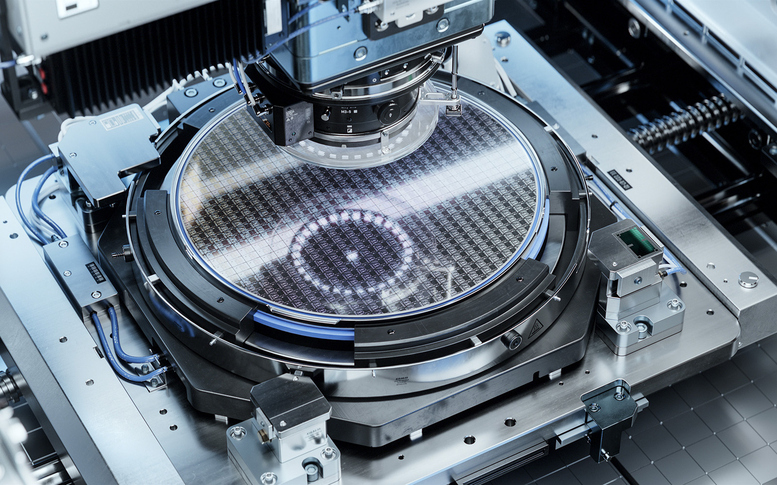
As demonstrated above, wafer manufacturing is the culmination of technologies spanning materials science, mechanical engineering, chemistry, and electronics, representing one of the most advanced industrial technologies in the world.
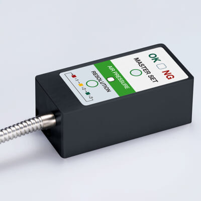
High-precision seating confirmation of workpiece and jig
- Air Gap Sensor -
You can check not only "presence/absence" but also "adhesion (gap)" at the same time with a repeatability of ±0.5 μm.
Click here ›Future Outlook for Semiconductor Wafers
As semiconductor demand continues to increase, the wafer industry is entering a period of major transformation. The following trends are attracting particular attention.
1. Larger Wafer Sizes
Following 300mm wafers, mass production of 450mm wafers is anticipated. Larger wafer sizes improve chip yield per wafer and enhance cost efficiency. However, large-scale upgrades to manufacturing equipment and production lines are required, demanding significant time and investment.
2. Emergence of Next-Generation Materials
In addition to conventional silicon, compound semiconductors such as SiC (silicon carbide), GaN (gallium nitride), and GaAs (gallium arsenide) are gaining attention. These materials offer excellent performance in high-voltage and high-temperature environments and are increasingly being adopted in power semiconductor and high-speed communication applications.
3. Use of Reclaimed Wafers
From an environmental perspective, the market for “reclaimed wafers,” which are reused after repolishing previously used wafers, is also expanding. Because they help reduce costs while maintaining quality, demand is growing particularly for testing applications.
4. Geopolitical Risks and Supply Chain Reinforcement
Semiconductor supply chains often depend heavily on specific regions or companies, raising concerns about geopolitical risks. In response, countries around the world are accelerating efforts to diversify manufacturing locations and bring production back domestically. In Japan as well, growth strategies leveraging the strengths of semiconductor material and equipment manufacturers are underway.
5. Commitment to Sustainable Development
Efforts toward carbon neutrality and green manufacturing are also becoming essential, driving the development of energy-saving manufacturing processes and recycling technologies for wastewater and chemicals.
Sensor Implementation Examples
Corrected thermal displacement of XY table in micron level
An inspection table (XY table) was being used in a semiconductor inspection process, but self-heating of the table over time caused micron-level displacement in the XY axes, making high-precision inspection difficult.
The use of a “Photomicro” sensor for XY-axis origin positioning was also considered, but its repeatability of 10μm was insufficient for micron-level correction.
The customer found our products through a keyword search for “thermal displacement” and “correction” and contacted us for assistance.
Resolved a false detection of the photo sensor under high-vacuum environment
This semiconductor manufacturing equipment manufacturer designs vacuum deposition equipment for producing semiconductors used in solar panels.
An engineer responsible for the substrate sensing section consulted us regarding the “positioning” of glass substrates in a vacuum environment. In the semiconductor industry, our sensors have also been widely adopted for positioning applications inside vacuum systems such as sputtering equipment, OLED deposition systems, etchers, and wafer transfer systems.
Wafer damage can be prevented by positioning with ±0.5μm repeatability
This semiconductor manufacturing equipment manufacturer produces “demounter systems” used to separate semiconductor wafers from substrates.
An engineer responsible for mechanical design consulted us regarding the “positioning” of the demounter drive section.